An alternative to the commodity accelerator solution for real-time control is to build tailored processor boards, based on high cell density FPGAs for instance, designed for the application and relying on custom data flow models. The great advantage of such approach is to provide full control over hardware and critical software (device driver) to ensure real-time and deterministic performance and to guarantee the support and availability of the solution over the system lifetime. However, this is usually done at the cost of an expensive and rather long development cycle (as compared to custom arithmetic designs) to produce specialized components with very few options for return on investment.
We believe that the emergence of new FPGA products, integrating an ARM-based Hard Processor System (HPS) with the FPGA fabric, could enable a new approach, merging the concept of compute node in a HPC cluster and specialized processor board in an application specific facility. Coupled to a comprehensive user-oriented development framework, including FPGA development environment and support for mainstream HPC tools and compilers, this new class of system-on-chip (SoC) could provide an energy efficient platform for HPC with a potentially wide application range.
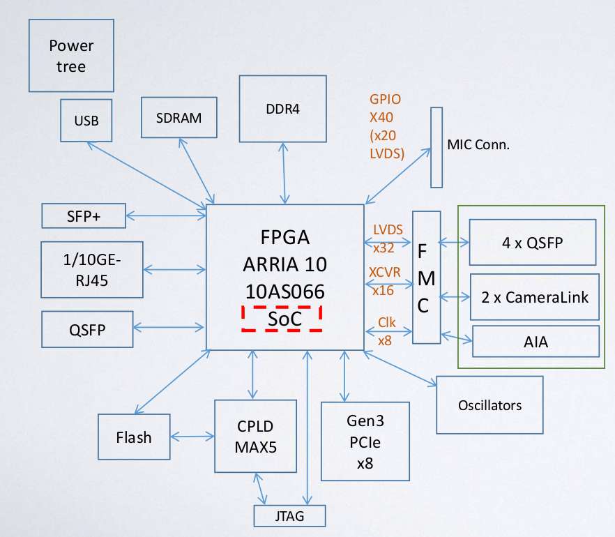
The primary objective of this axis of development is to prototype a main board, hosting a high cell density FPGA with an integrated ARM-based HPS, including a PCIe Gen3 rootport as an internal interface, and using 10G Ethernet and 40G Infiniband as network interface and back plane. (obj. 2.1)
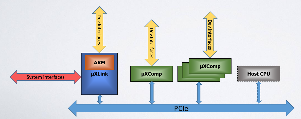
Another objective of this axis of development is to provide support for this prototype microserver in an integrated FPGA development environment (QuickPlay), deployable in the FPGA BSP and allowing to build a custom design on the FPGA, handling complex data flows through the internal (PCIe), the network interfaces and computing blocks, as well as the driver and end user API to use these features. Blocks developed in the first research axis on smart interconnects will be reused. (obj. 2.2)
The last objective of this axis of development is to build a small scale cluster by interconnecting several prototype microservers through a standard network protocol (10G Ethernet and 40G Infiniband). The performance achieved for the MVM algorithm and more generally the AO control application on single and multiple boards configurations will be assessed in terms of performance, determinism and energy efficiency as compared to an accelerator based solution. (obj 2.3)